Description
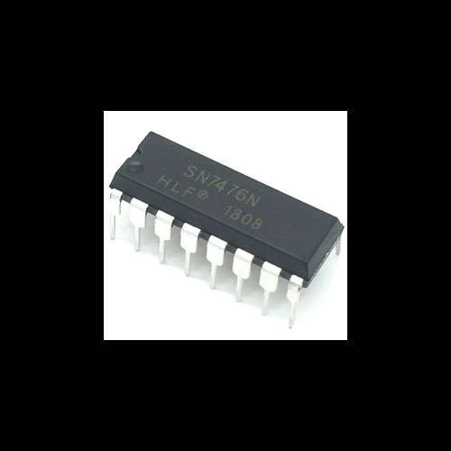
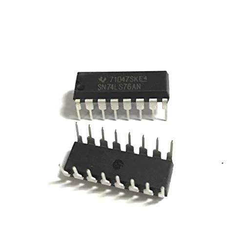
This device 7476 contains two independent positive pulse triggered J-K flip-flops with complementary outputs. The J and K data is processed by the flip-flop after a complete clock pulse. While the clock is LOW the slave is isolated from the master. On the positive transition of the clock, the data from the J and K inputs is transferred to the master.
While the clock is HIGH the J and K inputs are disabled.
Features
1. Output Drive Capability: 10 LSTTL Loads
2. Outputs Directly Interface to CMOS, NMOS and TTL
3. Operating Voltage Range: 2 to 6V
4. Low Input Current: 1mA
5. High Noise Immunity Characteristic of CMOS Devices
6. In Compliance With the JEDEC Standard No. 7A Requirements
7. Chip Complexity: 100 FETs or 25 Equivalent Gates









Reviews
There are no reviews yet.